In the precision arena of lithography machines, dual stages play a crucial role in achieving efficient and accurate lithography. Imagine it as a skilled dancer gracefully performing on a microscopic stage, expertly transporting the silicon wafer through the intricate exposure process.
1. The suspension mode of the workpiece table: The evolution from mechanical to magnetic levitation has transformed the way silicon wafers are handled. For optimal lithography quality, the workpiece table must enable the silicon wafer to move quickly and stably. The performance of the workpiece table—encompassing speed, acceleration, and positioning accuracy—is directly linked to the quality of the lithography. The suspension mode has undergone several generations of technological advancements to enhance these capabilities.
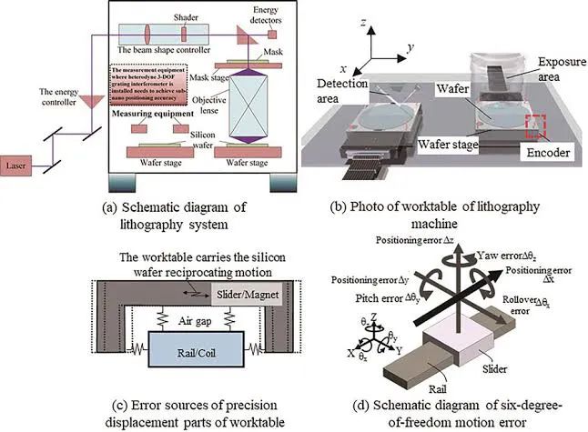
(1) Mechanical Guide Rail Type: The earliest workpiece tables that began “staggering” operated using mechanical guide rails. However, the machining accuracy of the bearings was limited, with positioning accuracy generally reaching no better than 1 μm. Additionally, mechanical friction generated heat and was prone to contamination, which made this technology inadequate for semiconductor manufacturing that demands higher precision. As a result, it was gradually replaced by more advanced technologies.
(2) Air Suspension Workpiece Table: To address the issues associated with mechanical contact, the air suspension workpiece table was developed. This design employs an “air cushion” created by gas, which eliminates direct contact between the workpiece table and the base, significantly reducing friction. With an integrated measurement and control system, the scanning speed increases, and accuracy can be achieved below 100 nm, thereby meeting some of the lithography requirements for precision and speed.
(3) Magnetic Levitation Workpiece Table: As technology advanced, the need for higher output and speed intensified, leading to the demand for lighter workpiece tables with improved motion performance.
The NXT 1950i lithography machine, launched by ASML in 2008, features a combination of a lightweight chemical structure table, a magnetic levitation system, and a planar grating scale positioning system. This design reduces the weight by approximately two-thirds compared to the air suspension platform, while achieving motion accelerations of up to 5G.
The latest generation of lithography technology has achieved an acceleration of 7G, with positioning accuracy as precise as 1 nanometer and scanning speeds of up to 800 mm/s. These advancements significantly enhance lithography efficiency.
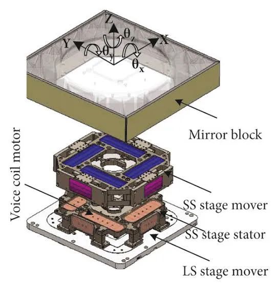
In EUV lithography systems, maintaining a high vacuum environment necessitates the use of magnetic levitation (maglev) workpiece tables. For instance, the ASML double-stage lithography machine features two stages for workpiece handling: a long-range stage (macro stage) and a short-range stage (micro stage).
The long-range stage is responsible for movements in the micrometer range and above, such as station exchange and scanning exposure. After the long-range stage has moved, the short-range stage performs nano-level fine-tuning, which includes compensating for overlay and adjusting focal length during exposure.
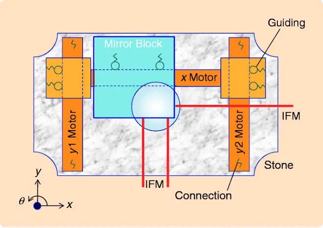
The maglev platform consists of a permanent magnet (stator) and an energized coil (mover), driven by a two-dimensional planar motor. It typically includes at least six sets of current-carrying coils to accommodate six degrees of freedom. The long-range stage often employs a “moving coil without moving iron” structure, with a magnetic array arranged in the Halbach configuration. The force acting on the long-range platform depends on its position within the magnetic array and the direction of the current from the three-phase alternating current supply.
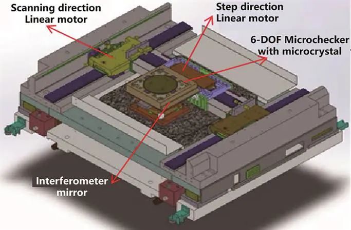
When the system is at rest, the vertical force maintains suspension. During movement, the phase and intensity of the three-phase alternating current are adjusted corresponding to different positions, working with the motor driver to achieve translation along the X, Y, and Z axes, as well as rotation around these axes (Rₓ, Rγ, Rz).
Similarly, the short-range stage also requires precise positioning, often using air levitation or magnetic levitation, and is driven by a Lorentz motor or Halbach permanent magnet. This setup connects the long-range stage to the silicon wafer, ensuring nanometer-level adjustment accuracy.2. The structure and working principle of the double workpiece table: the synergy of efficiency and accuracy
(1) From single to double: the “jump” of production capacity
In the early stage of the single workpiece table lithography machine, when the silicon wafer and the reticle are leveled and aligned, the exposure equipment has to be “idle” and wait, wasting production capacity. The advent of double workpiece tables makes it possible to operate in parallel.
ASML’s double-stage lithography machine was launched in 2000, and in 2001 the first KrF lithography machine with a two-stage AT 750T was delivered, and since 2004 it has been extended to the XT series (air suspension) of water immersion lithography machines.
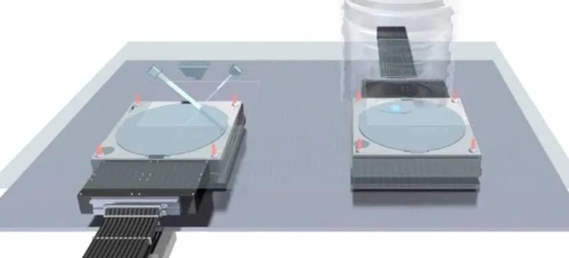
It has two workpiece tables, each containing a micro-motion table and a macro-motion table, which are respectively at the measurement station and the exposure station, and are suspended on the marble substrate by a three-phase four-pole permanent magnet synchronous motor.
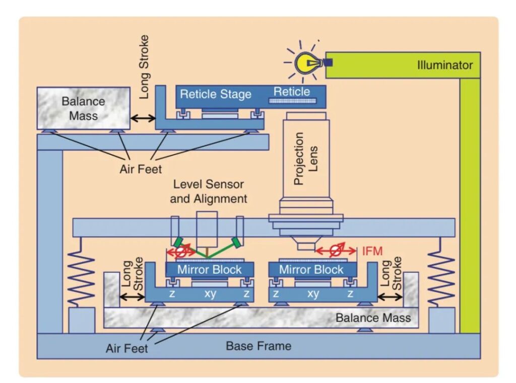
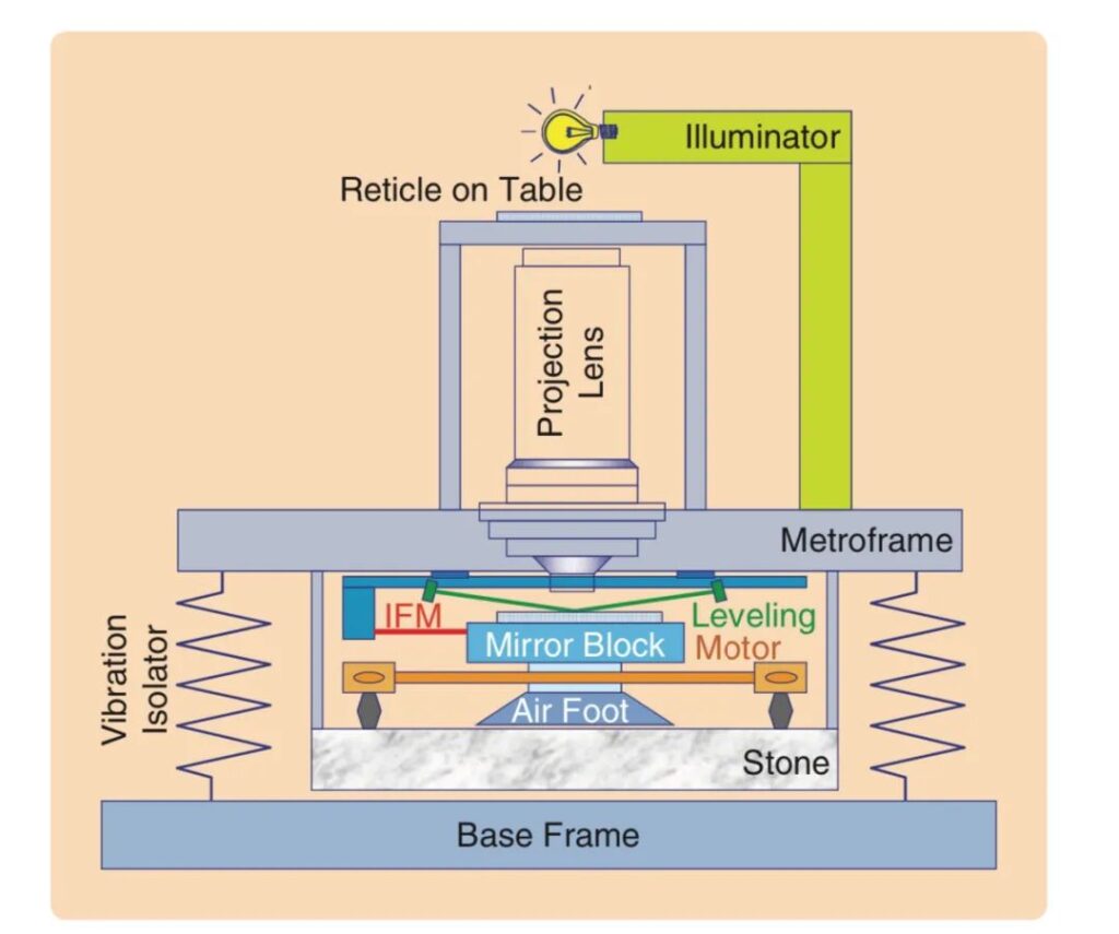
There is a measuring microscope and focusing and leveling equipment above the measuring station; There is a projection objective above the exposure station. Together with the measurement and control system (laser interferometer or planar grating scale), these devices are fixed to the measuring bracket and are in no contact with the workpiece table. In this way, when the measuring station is used for silicon wafer alignment, focusing and alignment, the exposure station can be synchronized with exposure, which greatly increases the production capacity of the lithography machine.
Workflow:Before the alignment and exposure process, the silicon wafer must be aligned and leveled. The alignment involves positioning the front mark on the silicon wafer with the mask mark in both the X and Y directions. Focus leveling is needed to align the reticle with the silicon wafer in the Z direction.
1. Alignment Method: There are two primary methods for aligning the silicon wafer with the reticle: Through-The-Lens (TTL) alignment and Off-Axis (OA) alignment, which is also known as indirect alignment. TTL can complicate lens design and limit the accuracy and wavelength of alignment. Consequently, advanced lithography machines often utilize indirect alignment.
2. Focus and Leveling: A multi-layer “check” is employed to ensure accurate leveling. This involves using a wide band of visible, infrared, or ultraviolet light in a grazing incidence mode. A total reflection telecentric imaging device projects a grating image onto the surface of the silicon wafer. The reflected image is then projected onto the detection grating through another device, which is modulated by an electronically controlled vibration element to obtain an AC signal. This allows for the calculation of the Z direction of the silicon wafer. During exposure, the horizontal and vertical positions of the workpiece table are dynamically adjusted to keep the silicon wafer as close to the best focal plane of the lens as possible.
However, the penetrating visible-infrared light can be affected by the substrate material, impacting measurement accuracy. To address this, ASML employs a barometric pressure sensor, which, while slower, offers accurate measurement of the wafer’s surface undulation. This is combined with the visible-infrared light leveling device to balance speed and accuracy. Later, UV Leveling was developed, using 200-425 nm ultraviolet light to provide leveling data that is closer to the surface of the silicon wafer, enhancing accuracy due to the shallow penetration of ultraviolet light.
After entering the lithography machine, the silicon wafer must undergo the following steps for preparation:
– **Pre-Alignment: Locate the silicon wafer notch (Notch) at the measurement station. The accuracy in the X and Y directions is approximately ±10 μm, which is the conventional level for mechanical positioning without closed-loop control.
Coarse Leveling: This step involves flattening the edges along the wafer and achieving a macro-level of the wafer. Due to a height difference of about 1 μm between the center and the edges of the silicon wafer, the coarse leveling accuracy in the Z direction is approximately ±1 μm.
Coarse Alignment: After the initial coarse leveling, use an alignment microscope (with a wavelength range of 550 – 750 nm and numerical aperture (NA) of 0.3) to image the alignment marks in the exposure field. Based on the depth of focus formula, the depth of focus is approximately ± (3 – 4) μm. This means that the coarse leveling accuracy falls within this depth of focus, allowing for quick imaging without the need for refocusing. The coarse alignment accuracy in the X and Y directions is about ±3 μm.
Fine Leveling and Fine Alignment: To further enhance accuracy, we aim for a precision of ± (5 – 10) nm in the Z direction and ± (1 – 2) nm in the X and Y directions. The system then uses an interferometer measurement and control system for closed-loop control, ensuring high precision is maintained.
Exposure Station Exchange: The workpiece table is shifted to the exposure station, where the reticle and workpiece table (with a transmission pattern sensor) are aligned before the exposure process begins.
The “parallel magic” of the dual workpiece stage allows for simultaneous execution of silicon wafer alignment, focusing, leveling, and exposure. For example, silicon wafer station 1 aligns and levels silicon wafer A at the measurement station while silicon wafer table 2 exposes silicon wafer B at the exposure station. After silicon wafer B is exposed, the positions of the two workpiece tables are exchanged via the measurement and control position of the plane grating or laser interferometer. Then, silicon wafer station 2 receives a new silicon wafer C, aligns and levels it at the measurement station while silicon wafer A on table 1 is exposed at the exposure station. This cycle significantly increases the utilization of expensive lenses and the capacity of the lithography machine.
Clever Coordination of Indirect Alignment: The transmission image sensor on the silicon wafer table acts as the “ferryman.” First, we use the alignment microscope to image the alignment marks in the multiple exposure fields of the silicon wafer (using either Nikon brightfield or ASML darkfield mode) at the measurement station and record the spatial relationship between the marks and the sensor. Once the workpiece table reaches the exposure station, the alignment mark (grid) on the reticle plate aligns with the sensor grid through the projection objective lens, allowing the sensor to detect maximum light intensity. This step completes the alignment of the reticle and the workpiece table in the X, Y, and Z directions, indirectly achieving the alignment of the silicon wafer and the reticle while also recording the position coordinates for exposure.
This indirect alignment approach eliminates the need to consider both the aberration of the alignment light source and the exposure light source simultaneously, thereby reducing the complexity and cost of lens design. Additionally, it broadens the alignment wavelength range, continuously improving alignment accuracy.
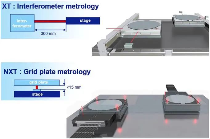
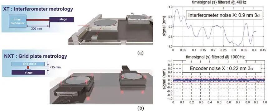
(3) Measurement and Control System: After the key lithography process, precise navigation, overlay, and line width must be measured. As the workpiece table moves, the measurement and control system must accurately track its position. This system has evolved from the traditional six-channel laser interferometer to a four-piece spliced plane grating scale used in the 193nm water immersion lithography machine.
Traditional laser interferometers measure position but must compensate for changes in the refractive index of air; otherwise, measurement noise and errors occur. ASML’s planar grating scale for advanced double-stage lithography machines reduces the impact of air disturbances. Due to the vacuum environment, EUV lithography machines can effectively utilize low-cost traditional laser interferometric measurements.
Although traditional laser interferometers are economical and easy to manufacture, air disturbances can compromise measurement accuracy. When the workpiece table changes positions, the original laser beam cannot be tracked, necessitating a re-determination of its position (using grating rulers, zero sensors, etc.), which increases exchange time and affects production efficiency. The combination of flat grating scales and relay grating scales allows for continuous tracking of the workpiece table’s position and enhances the exchange speed between the two workpiece tables.
(4) Performance Parameters Affecting Line Width and Overlay:** When assessing accuracy, two key movement parameters of the workpiece table significantly influence chip yield: Moving Average (MA) and Moving Standard Deviation (MSD). MSD indicates the high-frequency elements of positioning error, while MA represents the low-frequency components. As technology advances, particularly at smaller nodes, high-resolution lithography patterns show a close correlation with MSD. An increase in MSD leads to reduced pattern contrast and blurriness, thereby affecting line width uniformity. At the 180nm technology node, MSD is approximately 20nm, while in the 193nm water immersion lithography machine, it drops to about 6nm.
Overlay accuracy is constrained by MA. In dual-pattern technologies, overlay accuracy must be less than 10% of the line width, necessitating a reduction in MA. For instance, to achieve a lithography pattern with a half-period of 38nm, the MSD must be below 6nm, overlay accuracy should be around 4nm, and the corresponding MA must be less than 1nm. With advancing technology nodes, the requirements for line width uniformity and overlay precision continue to rise, necessitating ongoing improvements in the performance of the workpiece table to meet the demands of mass production.
3. Conclusion:** As the most sophisticated and expensive equipment in semiconductor manufacturing, the development of double workpiece stages exemplifies the progress in lithography technology. From advancements in suspension modes to structural and operational optimizations, and to stringent controls on measurement and performance parameters, every advancement contributes to the continual reduction of integrated circuit line widths.
As technology nodes progress, lithography equipment, materials, and methods continually evolve. The “precision dancer” role of the double workpiece stage enables silicon wafers to perform complex exposure actions on a micro scale, offering significant support for the efficiency and accuracy of chip manufacturing and heightening our anticipation for the future of semiconductor technology.