In the core of the semiconductor industry, chip manufacturing plants are renowned for their high level of automation, ultra-clean environment, and complex technological processes. These plants are not only symbols of technology-intensive industries but also paragons of precision engineering and spatial design.
I. Precise Division of Manufacturing Areas
(I) Thin Film Area: Laying the “Foundation” of Chips
The thin film area is the starting point of chip manufacturing. Its core task is to deposit various functional thin film materials on the surface of wafers. These films include insulating layers, conductive layers, and semiconductor layers, which serve as the basis for subsequent processes.
- Physical Vapor Deposition (PVD)
The PVD area mainly deposits metals or metal compounds onto the wafer surface through physical methods. Take magnetron sputtering as an example. Argon ions are accelerated by an electromagnetic field to bombard the target material, causing the atoms of the target material to sputter and deposit on the wafer. This technology is widely used to form key structures such as metal gates and diffusion barriers, featuring high deposition rates and precise composition control. For instance, in advanced manufacturing processes, the deposition of TiN metal hard masks relies on magnetron PVD technology. - Chemical Vapor Deposition (CVD)
The CVD area generates thin films on the wafer surface through chemical reactions. Plasma – Enhanced Chemical Vapor Deposition (PECVD) can deposit dielectric layers such as silicon nitride at relatively low temperatures, which are used for passivation and insulation. Low – Pressure Chemical Vapor Deposition (LPCVD) is suitable for growing high – quality polysilicon thin films, which are used as the active region material for transistors. For example, in 3D NAND flash manufacturing, LPCVD is used to grow high – aspect – ratio silicon dioxide layers.
(II) Lithography Area: Nanoscale “Light and Shadow Engraving”
The lithography area is a core link in chip manufacturing. Its function is to transfer the designed circuit pattern onto the wafer. The photoresist undergoes a chemical reaction when irradiated by light of a specific wavelength, thereby forming an accurate pattern.
- The Mystery of Yellow Lights
The lithography area is illuminated by yellow lights with a wavelength of 570 – 620nm. This is because the photosensitive range of the photoresist is concentrated in the ultraviolet and blue light bands of 200 – 500nm. Yellow lights can provide the visibility required for operations while avoiding accidental exposure of the photoresist. In addition, the yellow spectrum can also reduce glare on the surface of equipment, improving the visual comfort of operators. - Challenges of the Lithography Process
As the manufacturing process nodes enter the nanoscale range, the difficulty of lithography has increased significantly. For example, Extreme Ultraviolet Lithography (EUV) uses a wavelength of 13.5nm, which requires precise control of the stability of the light source and the accuracy of the optical system. The cleanliness requirements in the lithography area are extremely high, usually reaching ISO Class 1, to avoid particle contamination affecting pattern resolution.
(III) Etching Area: The “Nanoscale Scalpel” for Precise Removal
The task of the etching area is to remove the unnecessary materials on the wafer surface through physical or chemical methods to form precise three – dimensional structures.
- Dry Etching and Wet Etching
Dry etching uses ions in the plasma to bombard the wafer surface, featuring high selectivity and controllability, and is widely used in the processing of high – aspect – ratio structures. Wet etching dissolves materials through chemical solutions and is suitable for large – area uniform etching. For example, in FinFET manufacturing, dry etching is used to form fin – like structures, while wet etching is used to remove photoresist residues. - Key Technologies of Etching Equipment
Etching machines need to precisely control the density, energy, and uniformity of the plasma. For example, Reactive Ion Etching (RIE) achieves selective etching of different materials by adjusting the radio – frequency power and gas flow. Advanced etching equipment is also integrated with in – situ monitoring technology to provide real – time feedback on the etching depth and uniformity.
(IV) Ion Implantation Area: The Doping Process that “Endows the Soul” to Semiconductors
The ion implantation area introduces impurity atoms into the wafer surface through high – energy ion beams, changing the electrical properties of the semiconductor.
- The Working Principle of Ion Implantation Machines
Ion implantation machines consist of an ion source, an acceleration tube, and a scanning system. The ion source generates the required ions (such as boron and phosphorus), the acceleration tube accelerates the ions to energies ranging from several tens of keV to several hundreds of keV, and the scanning system ensures the uniform distribution of ions on the wafer. For example, low – energy high – current ion implantation machines are used to form shallow junctions, while high – energy ion implantation machines are used for deep – buried layer doping. - Challenges of Precise Control
The dose, energy, and angle of ion implantation directly affect device performance. For example, in FinFET manufacturing, precisely controlling the dose and depth of Halo doping can effectively suppress the short – channel effect. To reduce wafer damage, advanced ion implantation machines also adopt dynamic annealing technology, which heats the wafer in real – time during the implantation process.
(V) Furnace Tube Area: Material Modification in a High – Temperature Environment
The furnace tube area uses a high – temperature environment to carry out processes such as oxidation, diffusion, and annealing to achieve material modification on the wafer surface.
- Oxidation and Diffusion Processes
In a high – temperature furnace tube, a silicon wafer reacts with oxygen to form a silicon dioxide layer, which is used for gate insulation or device isolation. The diffusion process allows impurity atoms to diffuse into the wafer interior through high – temperature, forming a PN junction. For example, in the CMOS process, furnace tube oxidation is used to form the gate oxide layer, and its thickness can be precisely controlled within a few nanometers. - Key Temperature Control Technologies
The temperature control accuracy requirements in the furnace tube area are extremely high. Usually, multi – zone heating and closed – loop feedback systems are employed. For example, the temperature control accuracy of a certain PECVD device can reach ±1℃, and it also has a rapid cooling function to improve production efficiency. In addition, the use of dummy wafers can stabilize the gas flow and temperature in the furnace tube, reducing particle defects on product wafers.
(VI) Chemical Mechanical Polishing (CMP) Area: The “Magic” for Achieving Global Planarization
The CMP area combines chemical corrosion and mechanical grinding to remove the high points on the wafer surface and achieve global planarization.
- The Principle of the CMP Process
The wafer is fixed on a rotating suction cup and comes into contact with a polishing pad coated with a polishing slurry. The abrasive particles (such as silicon dioxide) in the polishing slurry remove materials through mechanical action, while chemical reagents promote surface chemical reactions to form a soft layer that is easy to remove. For example, in the multi – layer metal interconnection process, CMP is used to planarize the metal wiring layer to ensure the accuracy of subsequent lithography. - Innovations in Polishing Pads and Polishing Liquids
Companies such as 3M have developed CMP polishing pads using micro – replication technology, optimizing the grinding efficiency and surface flatness. The oxidants and catalysts in the polishing liquid can be customized according to different materials. For example, acidic polishing liquids are used for copper interconnections, and alkaline polishing liquids are used for tungsten plugs.
II. Intelligent Design of Factory Structures
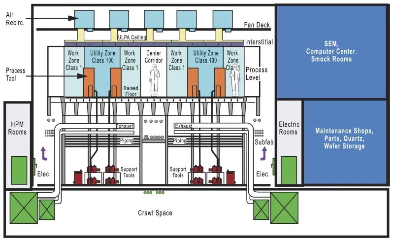
(I) Raised Floor: The “Invisible Passage” for Airflow and Pipelines
The raised floor is a structure of semiconductor factories. Its opening design and the space below it serve multiple functions.
- The Function of Openings
The opening rate of the raised floor is usually 10% – 20%, mainly used for the return air system. The Fan Filter Units (FFUs) at the top of the clean room vertically send clean air downward. The air passes through the openings and enters the return air passage below the floor, forming a vertical unidirectional flow to ensure air cleanliness. In addition, the openings are also used for the routing of cables and process pipelines, avoiding the impact of ground pipelines on production operations. - The Sub – Fab Below the Floor
The Sub – Fab is an auxiliary area below the raised floor, integrating various support systems. For example, dry vacuum pumps are used to maintain the vacuum environment of the process chambers, the cooling water system provides constant – temperature cooling for equipment, and the chemical delivery system precisely distributes the gases and liquids required for the process to each machine. The design of the Sub – Fab needs to consider the spatial layout and maintenance convenience. For example, modular design is adopted to facilitate the rapid replacement of faulty equipment.
(II) Fresh Air System: The “Source of Life” for Clean Air
The fresh air system is responsible for providing filtered fresh air to the clean room while maintaining the balance of temperature, humidity, and air pressure.
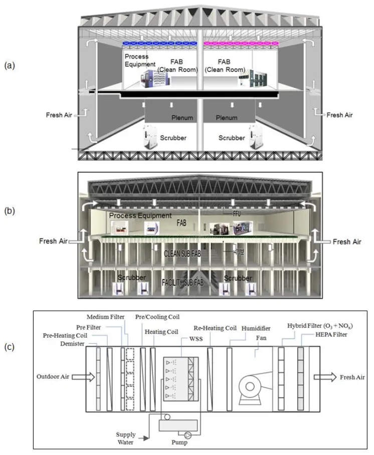
- Multi – Stage Filtration and Airflow Control
Fresh air first passes through a primary filter to remove large – particle dust, and then through medium – and high – efficiency filters (HEPA/ULPA) to filter particles above 0.1μm. Chemical filters are used to remove gaseous pollutants (AMC), such as acids, alkalis, and organic compounds. The FFUs adjust the wind speed through frequency conversion control to ensure that the air flow speed in the clean room is stable at 0.45m/s ± 20%. - Energy – Saving and Environmental – Friendly Design
Advanced fresh air systems adopt heat recovery technology, using the heat of the exhaust air to pre – heat the fresh air and reduce energy consumption. For example, the fresh air system of a certain semiconductor factory building can recover 70% of the exhaust heat through a plate – type heat exchanger, saving several million yuan in electricity bills annually.
(III) Clean Rooms and Corridors: Balancing Cleanliness and Efficiency
Clean rooms are the core areas of chip manufacturing. Their design needs to balance cleanliness and production efficiency.
- Cleanliness Classification and Area Division
According to SEMI standards, clean rooms are usually divided into Class 1 to Class 10. Among them, Class 1 has the highest cleanliness level, with no more than 10 particles of 0.1μm per cubic meter of air. Key processes such as lithography and ion implantation are carried out in Class 1 or Class 2 clean rooms, while auxiliary areas such as dressing rooms and material storage rooms are Class 100 or lower. The corridors, as channels for personnel and materials, use differential pressure control to prevent the spread of pollution. For example, the differential pressure between the clean room and the corridor is maintained at 5 – 10Pa. - Material Transfer and Personnel Routes
Materials enter the clean room through transfer windows or automated logistics systems (such as AGVs) to avoid air flow disturbances caused by frequent door openings. Personnel need to pass through air showers to remove dust on their clothing surfaces and wear clean suits, gloves, and masks to ensure their own cleanliness.
(IV) Ceiling System: The “Aerial Fortress” of FFUs and Filters
The ceiling system is located above the clean room and integrates FFUs, ULPA filters, and chemical filters. It is the key to maintaining a clean environment.
- High – Efficiency Filtration of FFUs
FFUs consist of fans and filters. They provide clean air to the clean room through self – circulation. The rated air volume of each FFU is 900 – 1200m³/h, which can cover an area of approximately 1.5 – 2 square meters. The filtration efficiency of ULPA filters can reach 99.999% @ 0.12μm, ensuring that ultra – fine particles in the air are effectively intercepted. - The Supplementary Role of Chemical Filtration
For AMC pollutants, the chemical filters (such as activated carbon or zeolite) in the ceiling system can adsorb acids, alkalis, and organic gases. For example, in the lithography area, chemical filters can remove the organic vapors volatilized from the photoresist to prevent them from contaminating the wafer surface.
(V) Exhaust System in Sub – Fab: The “Environmental Guardian” for Waste Gas Treatment
The Exhaust system is responsible for collecting and treating the waste gases generated during the manufacturing process to ensure environmental safety.
- Waste Gas Classification and Treatment Technologies
- Acidic and Alkaline Waste Gases: They are neutralized by washing with water in a scrubber. For example, sodium hydroxide solution is used to treat acidic waste gases.
- Toxic Waste Gases: They are first preliminarily treated by the Local Scrubber 自带的机台 and then sent to the Central Scrubber for deep purification.
- Organic Solvent Waste Gases: A zeolite concentration rotary wheel + incinerator is used, with a removal rate of over 90%.
- General Waste Gases: They are directly discharged, but the concentrations of particulate matter and volatile organic compounds (VOCs) need to be monitored.
- Pipeline Materials and Safety Design
Corrosive waste gases use stainless – steel pipes lined with Teflon, and flammable waste gases use fire – resistant materials. The main pipeline is equipped with an automatic sprinkler system to prevent the spread of fire. In addition, the Exhaust system is also integrated with real – time monitoring sensors. Once abnormal concentrations are detected, an emergency treatment procedure is immediately triggered.
(VI) Lighting System: The “Precise Collaboration” of Yellow Lights and Clean Room Lights
The lighting system not only provides illumination but also needs to meet cleanliness and process requirements.
- The Special Mission of Yellow Lights
The yellow lights in the lithography area use a spectrum of 570 – 620nm to avoid exposing the photoresist. Their design needs to ensure no ultraviolet leakage. For example, special filter films or LED light sources are used. The illuminance of yellow lights is usually 200 – 300lx, which not only ensures operation visibility but also reduces eye irritation. - Design Standards for Clean Room Lights
The general lighting in clean rooms uses LED or fluorescent lights with an illuminance of 300 – 500lx. The lamps need to be embedded in the ceiling and sealed to prevent dust accumulation. For example, teardrop – shaped lamps, due to their streamlined design, can reduce air flow disturbances and dust adhesion. Emergency lighting and evacuation indicators use explosion – proof LED lights to ensure normal operation in case of emergencies.
III. The Core Logic of Factory Design
The layout and structure design of semiconductor chip manufacturing plants always revolve around two core goals: ensuring cleanliness and optimizing production efficiency. From the precise deposition in the thin – film area to the nanoscale engraving in the lithography area, from the air – flow control of the raised floor to the waste – gas treatment in the Sub – Fab, every link reflects the ultimate pursuit of details. This design is not only the crystallization of technology but also the embodiment of engineering wisdom, ensuring high – quality chip manufacturing at the nanoscale. In the future, with the continuous progress of manufacturing technologies, the design of semiconductor factories will continue to innovate to meet more complex process challenges and stricter environmental requirements.
Hey there!
Welcome to Moviezhive.com, where blockbuster entertainment is just a click away!
Stream a vast collection of Bollywood, Hollywood, and international movies for free—no subscriptions, no hassles.
What Makes Us Special?
✔️ Thousands of movies across all genres
✔️ Zero pop-up ads for seamless viewing
✔️ Advanced zero-buffering tech for smooth playback
✔️ Fresh titles added regularly
Can’t find a movie? Request it, and we’ll upload it fast!
Watch anytime, anywhere. Visit https://moviezhive.com now and start your movie adventure!
Enjoy the Show,
The Moviezhive Team