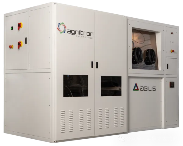
MOCVD Equipment and Process Introduction
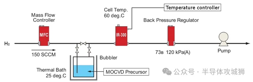
In MOCVD thin film growth, a carrier gas passes through a metal reaction source container (bubbler) to evaporate the precursor, carrying the saturated vapor of the reaction source into the reaction chamber to mix with other gases. The chemical reaction then occurs on the heated substrate to grow the thin film. Hydrogen is typically used as the carrier gas, though nitrogen is used in some special processes (e.g., for growing Indium Gallium Nitride (InGaN) films).
Bubbler and Evaporated Precursors
Commonly used substrates include Gallium Arsenide (GaAs), Gallium Phosphide (GaP), Indium Phosphide (InP), silicon, Silicon Carbide (SiC), and Sapphire (Al₂O₃). The grown thin films are primarily III-V compound semiconductors (such as GaAs, Aluminum Gallium Arsenide (AlGaAs), Aluminum Gallium Indium Phosphide (AlGaInP), InGaN) or II-VI compound semiconductors. These semiconductor thin films are applied in optoelectronic devices (e.g., Light-Emitting Diodes (LEDs), Laser Diodes (LDs), solar cells), microelectronic components (e.g., Heterojunction Bipolar Transistors (HBTs)), and Pseudo-Morphic High Electron Mobility Transistors (PHEMTs).
Component Introduction
The MOCVD system consists of a reaction chamber, a gas control and mixing system, reaction sources, and an exhaust gas treatment system.
Composition of the MOCVD System
- Reaction Chamber
- The outer wall of the chamber is typically made of stainless steel, while the inner wall is lined with quartz, graphite, or high-temperature-resistant ceramics (such as silicon carbide).
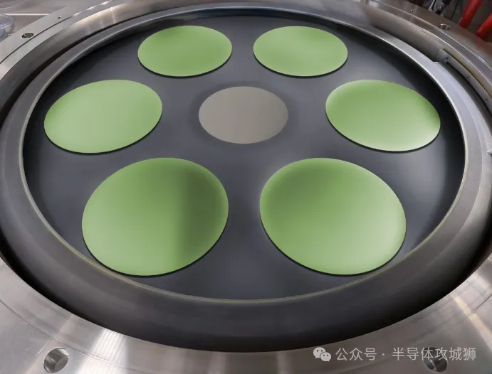
- A carrier disk inside the chamber holds the substrate. The carrier disk efficiently absorbs energy from the heater to reach the temperature required for thin film growth without reacting with the process gases.
- Heaters can be installed inside the chamber (e.g., metal resistance wires, graphite heaters) or outside (e.g., infrared lamps for quartz chamber walls, microwave heating).
- Cooling water channels are present on the outer wall and sealing areas of the chamber to prevent overheating during thin film growth.
- The central nozzle is positioned below the carrier disk, with gases ejected horizontally from the nozzle. The substrate is placed on the carrier disk above the central nozzle. If the central nozzle were above the substrate, reaction by-products might contaminate the thin film, even in trace amounts, reducing the final device performance.
- A single carrier disk can hold multiple substrates (wafers). To ensure uniform film thickness, the carrier disk and substrates can rotate (at speeds up to 1500 RPM) via a mechanical gear structure.
- The heater above the substrate can reach temperatures up to 1500°C. Multi-zone temperature control via multiple heater groups ensures nearly uniform temperature across the substrate, guaranteeing thickness uniformity.
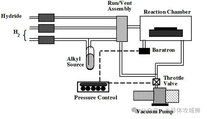
- Gas Control and Mixing System
- Carrier gas flows from the facility utility end through a gas switching system comprising manual valves, pressure reducers, pressure gauges, filters, Mass Flow Controllers (MFCs), and diaphragm valves. This system determines the gas flow direction, such as for participating in thin film growth reactions, purging by-products, or providing an inert gas environment.
- MOCVD processes typically operate near atmospheric pressure. The pressure, flow rate of different gases, and substrate temperature must be adjusted, as these factors affect thin film growth rate, thickness uniformity, and defect density. Optimal thin film growth requires continuous process parameter optimization.
- Reaction Sources
- Reaction sources are categorized into two types: metal-organic reaction sources and hydride gas sources, both of which are toxic and stored in sealed stainless steel tanks.
- Metal-organic sources oxidize upon contact with air and have lower toxicity, while hydrides are highly toxic.
- Common metal reaction sources include Trimethylgallium (TMGa), Trimethylaluminum (TMAI), Trimethylindium (TMIn), Cyclopentadienyl Magnesium (Cp₂Mg), Diisopropyl Telluride (DIPTe), etc.
- Common hydrides include Arsine (AsH₃), Phosphine (PH₃), Ammonia (NH₃), and Disilane (Si₂H₆), etc.
- Exhaust Gas Treatment System (Scrubber)
- The exhaust system, located at the end of the process, adsorbs and treats all toxic gases passing through the system to reduce environmental pollution. Common scrubbers include dry, wet, and combustion types.
MOCVD Process for Growing GaN
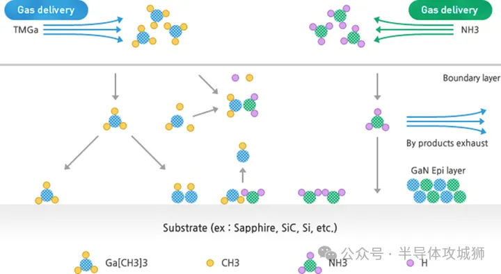
- Gas flows over a heated wafer (500–1500°C, material-dependent). Precursors like TMGa and NH₃ decompose when heated, releasing gallium and nitrogen atoms that grow GaN and bond to the substrate, extending layer-by-layer as the process proceeds.
- The MOCVD process enables alternating growth of different materials through rapid gas exchange in the reactor. For example, sequences of GaN and InGaN thin layers form the core of blue or white LEDs.