Metrology and Inspection in Semiconductor Manufacturing: ASML’s Influence
Semiconductor metrology and inspection are crucial for the semiconductor industry, directly impacting chip manufacturing precision and performance. ASML, the undisputed leader in semiconductor lithography, also holds significant influence in the metrology and inspection domain.
Overview of ASML
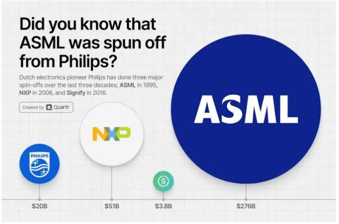
ASML was founded in 1984 as a joint venture between Philips and Advanced Semiconductor Materials International. In 1990, it spun off from Philips to become an independent company. Since its inception, ASML has focused on research and innovation in lithography technology, achieving a leading position through continuous technological breakthroughs and exceptional product performance.
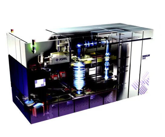
In 2001, ASML introduced the TWINSCAN system with its revolutionary dual-stage technology. This innovation allowed for the measurement and alignment of a new wafer while another was being exposed, significantly boosting system productivity and accuracy, thereby increasing customer value. This not only demonstrated ASML’s profound strength in technological research and development but also laid a solid foundation for its future growth.
In 2006, ASML released its first market-leading product, the TWINSCAN system utilizing immersion lithography. By introducing a layer of water between the lens and the wafer to project light, ASML successfully shortened the light source’s wavelength, enabling chip manufacturers to produce smaller chip features. This technological breakthrough solidified ASML’s dominance in lithography, maintaining its leading market share in high-end lithography machines.
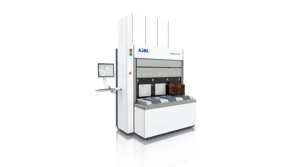
In 2008, ASML first launched the YieldStar (250D) system, which supported real-time test correction. This system provided real-time measurement and correction during the chip manufacturing process, further enhancing the precision and stability of lithography technology and advancing semiconductor manufacturing processes.
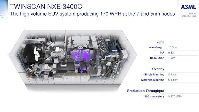
In 2010, ASML successfully launched the first prototype EUV lithography machine, NXE:3100, marking the dawn of a new era in lithography. EUV lithography technology uses light with shorter wavelengths, enabling the creation of much smaller chip features, which significantly boosted chip performance. Since then, ASML has continuously refined EUV lithography technology, becoming the sole manufacturer of EUV lithography machines globally, establishing an absolute monopoly in the high-end lithography market.
Beyond its outstanding achievements in lithography systems, ASML’s strategic focus in metrology and inspection equipment is closely integrated with its lithography systems. The goal is to reduce edge errors in every exposure step, ensuring consistency in overlay and critical dimensions, thereby improving chip manufacturing quality and yield.
ASML’s products primarily fall into two categories:
- Overlay error metrology based on optical inspection technology, mainly comprising the YieldStar series. In 2017, the YieldStar 375F began shipping. This system offered continuous wavelength selection between 425nm and 885nm, capable of measuring thousands of data points per batch, faster than previous solutions, allowing for precise optimization of measurement wavelengths and reduction of metrology costs. In 2021, the YieldStar 1385 series was introduced for post-etch pattern internal overlay error metrology, enabling multi-layer measurement in a single pass, further enhancing measurement efficiency and precision.
- Electron-beam defect inspection and electron-beam critical dimension metrology equipment based on electron inspection technology, including HMI eP5, HMI eScan600, HMI eScan 1000, and HMI eScan 1100. In 2022, the new-generation multi-electron beam defect inspection system HMI eScan 1100, equipped with 25 electron beams for continuous scanning, significantly increased throughput. In the same year, the eP5 XLE, a high-resolution system with a minimum resolution of 1nm, was released, primarily for inspecting and measuring 3D structures within logic and memory chips.
Patent Application Trends
Global Application Trends
ASML holds 264 global patents in key branches of metrology and inspection, including 23 transferred patents. Its global application trend can be divided into three phases:
- Initial Phase (before 2006): ASML’s patent applications began in 1996, but no patents were filed between 1997 and 2000. Upon review, the 1996 patent (US6166808A) was originally filed by Philips Electronics North America and was not independently developed by ASML. ASML’s independent patent applications began in 2002. During this period, out of 22 patents, 6 were acquired through patent transfers (one each in 1996, 2001-2003, 2005-2006). In this phase, ASML was in a stage of technological accumulation and exploration, with a small number of patent applications, partially relying on patent transfers for technology acquisition.
- Development Phase (2007-2012): From 2007 to 2009, the application volume saw its first rapid increase. The introduction of the YieldStar (250D) system in 2008 partly fueled ASML’s R&D enthusiasm in metrology and inspection, driving patent application growth. In 2010, application volume rapidly declined. In 2011-2012, the annual application volume recovered to 5-6 patents. During this phase, ASML’s technological R&D showed fluctuations, with market demand and uncertainty in technological breakthroughs impacting patent applications.
- Growth Phase (after 2013): The application volume saw its second rapid increase, growing from 10 in 2013 to 34 in 2018, reaching its peak. This indicates that ASML continuously increased its R&D investment in metrology and inspection, with technological innovations constantly emerging, leading to a significant rise in patent applications.
Application Trends in China
ASML holds 212 patents in China, including 13 transferred patents. The trend in China is largely consistent with the global trend, but with a different starting time. Applications in China began in 2001, later than the global start in 1996. However, ASML’s first independently developed patent application, CN101520609A, entered the Chinese market in 2002, demonstrating ASML’s重视 of the Chinese market.
- Initial Phase (before 2006): The annual application volume was low (fewer than 4 patents), indicating a stage of technology introduction and preliminary market development.
- Development Phase (2007-2013): A peak in applications occurred in 2009, reaching 14. As the Chinese semiconductor market gradually developed, ASML increased its technological deployment and R&D investment in China.
- Rapid Growth Phase (after 2013): The highest peak in applications occurred in 2018, reaching 34. During this period, the Chinese semiconductor industry rapidly rose, with strong market demand. ASML actively protected its technological innovations and market share in China through patent applications.
While the application trend in China is generally consistent with the global trend, there are differences in specific branches. ASML has patent applications in all key branches of metrology and inspection, but primarily focuses on overlay error metrology, wafer defect inspection, photomask defect inspection, and critical dimension metrology, with overlay error metrology having the most applications. Film thickness metrology and 3D morphology metrology have fewer applications, accounting for only 3% and 2% of total applications, respectively. Differences in global and Chinese application volumes are mainly seen in the overlay error metrology and photomask defect inspection branches. Further comparison of these two branches’ global and Chinese application trends shows that the differences primarily occurred before 2014 and after 2021. The difference after 2021 is mainly due to most patent applications in this period being PCT applications that have not yet entered the Chinese national phase. This reflects ASML’s increased focus on patent布局 in the Chinese market after entering the rapid growth phase in 2014.
Changes in the global distribution of ASML’s main metrology and inspection branches over different periods show that ASML had an earlier布局 in overlay error metrology and photomask defect inspection, while wafer defect inspection布局 came later, around 2007. Before 2016, the main branches were overlay error metrology and photomask defect inspection. After 2016, with the growth in wafer defect applications, overlay error metrology and wafer defect inspection became the main branches, with photomask defect inspection and critical dimension metrology accounting for a smaller proportion. This shift is likely due to ASML’s acquisition of HMI (Hermes Microvision Inc.), a leading electron-beam inspection company, in 2016, which increased its R&D investment in wafer defect inspection. A year later, it launched the eP5 system, integrating technologies from both companies, which could provide high-throughput critical dimension (CD) metrology and defect inspection.
Patent Legal Status
ASML’s global patent applications total 2656, with 55% still in force, 20% in the examination phase, and 16% expired (mostly due to non-payment of annual fees, withdrawal, and expiration of term). This indicates that ASML’s overall patent application quality is high, its R&D achievements are well-protected legally, and ASML maintains good patent management practices, ensuring timely maintenance of valid patents.
Regarding ASML’s patent legal status in China, 59% are in force, 29% are in the substantive examination phase, 5% have terminated rights, 2% are in the publication phase, and only 5% have been withdrawn or rejected. This indicates that ASML’s patent applications in China are not only of high quality but also demonstrate continuity. The high grant rate signifies that ASML’s patented technologies have strong competitiveness and adaptability in the Chinese market, while continuous patent applications reflect ASML’s long-term strategic布局 and sustained investment in the Chinese market. Therefore, ASML will continue to influence the metrology and inspection market in China for a considerable period.
Patent by Region
ASML’s global patent shows that China, the United States, Europe, South Korea, and Japan are key countries and regions. These regions have developed semiconductor industries and strong demand for semiconductor metrology and inspection technologies. By strategically placing patents in these regions, ASML can better protect its technological innovations and enhance market competitiveness. Additionally, Israel and the Netherlands are also important patent countries and regions. As ASML’s headquarters, the Netherlands has a complete scientific research system and industrial foundation, and patent there helps ASML consolidate its technological R&D advantages. Israel also possesses unique innovation capabilities and market demand in semiconductor technology, and ASML’s patent in Israel reflects its global strategic vision.
Although ASML’s patent count is not outstanding in the metrology and inspection domain, it places significant importance on overseas market, especially in China and the United States. China is one of the largest semiconductor markets globally, with immense market potential and development space. ASML’s increased patent in China allows it to better meet the demands of the Chinese market and increase its market share. The United States is a hub of semiconductor technology innovation, with numerous leading semiconductor companies and research institutions. Patent in the U.S. helps ASML engage in technological cooperation and competition with U.S. companies, maintaining its technological leadership in the global semiconductor field.
Key Inventors
Inventors play a crucial role in technological development and patent application growth. To understand ASML’s inventor team, we further analyzed their profiles.
The top-ranked inventor is ARIE JEFFREY DEN BOEF, with 36 applications, accounting for 21% of the total applications by the top 14 inventors. The second and third-ranked inventors are WEI FANG and MAURITS VAN DER SCHAAR, with 21 and 20 patent applications, respectively. The total applications by the top three inventors account for 45% of the total applications by the top 14 inventors. This indicates that the top three inventors contribute significantly to ASML’s patent applications, and their R&D achievements play a key role in ASML’s technological innovation.
Analyzing the R&D collaboration network of the top ten primary inventors reveals two distinct R&D teams. One team, led by ARIE JEFFREY DEN BOEF, includes key R&D members such as MAURITS VAN DER SCHAAR, EVERARDUS CORNELIS MOS, and MOHAMED SWILLAM. The other team, led by WEI FANG, primarily includes ZHONGWEI CHEN. Collaboration within these teams is close, but there is a lack of cooperation between the two R&D teams.
To understand the reason for the lack of cooperation between the two R&D teams, we further examined the research branches of their main inventor members. The team led by ARIE JEFFREY DEN BOEF focuses on overlay error metrology, while the team led by WEI FANG focuses on wafer defect inspection. WEI FANG and ZHONGWEI CHEN were R&D personnel from HMI (Hermes Microvision Inc.), which ASML acquired. This is one of the reasons for the lack of cooperation between the two R&D teams, as their different research directions and technical backgrounds led to a lack of common research foundations and motivation for collaboration during R&D.
Furthermore, while the top two inventors, ARIE JEFFREY DEN BOEF and WEI FANG, have different primary technical focuses, they are involved in various key technical branches, demonstrating their outstanding and comprehensive individual R&D capabilities. The involvement of other team members in specific branches is relatively more focused. ARIE JEFFREY DEN BOEF’s earliest patent application dates back to 2004, and the latest to 2020, indicating over 17 years of service at ASML. WEI FANG’s earliest patent application dates to 2006, and the latest to 2020, indicating over 15 years of service at HMI and ASML. This also reflects the strong stability of ASML’s R&D team, especially its leaders. A stable R&D team helps accumulate technical experience, maintain continuity and innovation in R&D work, and provides a solid talent foundation for ASML’s technological development.
Key Patent Technologies
Overlay Error Metrology
A review of ASML’s patent applications in overlay error metrology, considering both citation frequency and inter-citation relationships, reveals ASML’s technology development roadmap in this area, involving improvements in three aspects: measurement systems, overlay marks, and calculation methods.
- Measurement Systems: These involve improvements in detection accuracy, such as improvements to detection beams (US7453577B2) and correction of scatterometer asymmetry (US7656518B2). Optimizing detection beams and scatterometers enables more accurate measurement of overlay errors, improving chip manufacturing precision. They also involve improvements in detection speed, such as quickly and efficiently obtaining images of targets (CN102483582B) and detecting asymmetry (EP3361315A1). Rapid image acquisition and asymmetry detection can shorten detection time and increase production efficiency.
- Overlay Marks: The focus is on designing marks (e.g., by optimizing spacing, orientation, or adding auxiliary marks) that can identify errors at different thresholds (US7898662B2, EP3401733A1). Optimizing overlay mark design allows for more precise identification of overlay errors, ensuring chip manufacturing quality. Reducing measured intensity peaks at the periphery of sub-targets (CN11138187A), among other things, further enhances the reliability and accuracy of overlay error metrology.
- Calculation Methods: These primarily involve improvements to the optical diffraction-based overlay error metrology (DBO) method, including model improvements and parameter optimization and correction. Continuously improving calculation methods and models allows for more accurate calculation of overlay errors, providing more precise guidance for chip manufacturing.
Among the patents involved in the overlay error technology development roadmap, US7791727B2 serves as the foundation for the entire technical development, with other patents built upon its improvements. US7791727B2 is a patent filed by ASML in 2004 and is currently still in force. It discloses a method and apparatus for angle-resolved spectroscopic lithography characterization, including the ability to simultaneously measure angle-resolved spectra for multiple wavelengths and perform immersion scatterometry and focus measurement methods for angle-resolved scatterometers. This patent provides an important theoretical and technical foundation for the subsequent development of overlay error metrology technology.
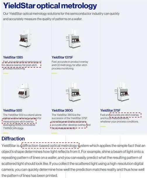
Products in the overlay error metrology field are mainly the YieldStar series:
- YieldStar 375F: Provides continuous wavelength operation, offering continuous wavelength selection between 425nm and 885nm. It can measure thousands of data points per batch, faster than previous solutions, allowing for precise optimization of measurement wavelengths and reduction of metrology costs. Key patents related to YieldStar 375F include US20070002336A1, NL2004216A, and CN109643068A. These patents protect key technologies of the YieldStar 375F, including wavelength selection and data measurement, ensuring the product’s technical advantages and market competitiveness.
- YieldStar 380G: The successor to YieldStar 375F, it provides faster and more accurate post-development overlay and focus metrology. The center wavelength selection is highly precise (1nm), and the bandwidth of the measurement light can be customized, with faster wavelength switching times and increased source power and faster sensors. Key patents related to YieldStar 380G include US7724370B2, CN113204173A, CN111736436A, EP3620857A1, WO2022111967A3, and EP4050328A1. These patents further optimize YieldStar 380G’s performance, such as improving wavelength selection accuracy and accelerating wavelength switching time, making it more accurate and efficient in metrology.
- YieldStar 500: An independent optical wafer metrology system for measuring pre-etch overlay. A new sensor design increases the system’s light transmission and reduces measurement acquisition time. Combined stage and sensor technology improves the platform’s throughput and overlay performance. Key patents related to YieldStar 500 include CN110914764A, CN114303100A, and CN115023658A. These patents innovate and protect aspects of YieldStar 500 such as sensor design and combined stage-sensor technology, enhancing the overall performance of the equipment.
- YieldStar 1375F: Based on the diffraction of the chip structure itself or small targets placed in the chip design, it can measure multiple layers simultaneously. The target is post-etch overlay and critical dimension (CD) metrology, capable of monitoring the performance throughout the chip manufacturing process. Key patents related to YieldStar 1375F include US7599064B2, US9915879B2, CN111338187A, and CN108292108B. These patented technologies enable YieldStar 1375F to perform multi-layer measurements, providing more comprehensive data support for monitoring the chip manufacturing process.
- YieldStar 1385: Used for post-etch overlay metrology of silicon wafers. This system can measure multiple layers at once through in-device chip features or small, dedicated metrology targets embedded in the chip design, helping to improve yield through post-etch process control. It integrates advanced machine learning technology, ensuring accurate measurements while remaining insensitive to other stack variations. Key patents related to YieldStar 1385 include EP3358413A1 and EP4134749A1. The application of machine learning technology further enhances measurement accuracy and stability, adapting to complex production environments.
Wafer Defect Inspection
Technology Development Roadmap
- Electron-based inspection: This is ASML’s primary development route in wafer defect inspection. It features high resolution but slow inspection speed. Therefore, the main development direction is to increase inspection speed, including using multiple electron beams for inspection and continuously moving the stage during inspection. Additionally, electron beam inspection also involves improving detection accuracy and effectiveness, including rotating the substrate around the central axis on an electrostatic chuck to the desired position to ensure inspection of all positions on bevels and vertices, and simultaneously collecting backscattered electron/secondary electron signals and released current signals and comparing these two signals to provide complementary information about the wafer structure, allowing for more accurate and effective detection of wafer structures without increasing wafer scanning time.
- Scattering-based inspection: ASML has fewer applications in scattering-based inspection compared to electron-based inspection. Its improvements primarily involve detection methods, such as determining whether defects are present from aligned first images and metrology images, and illuminating a measurement area of a structured surface with measurement light along at least two illumination beam paths having different angles of incidence relative to the surface normal. Additionally, improvements in scattering-based inspection also involve optical paths, such as improvements to high numerical aperture objective systems.
- Algorithms: ASML’s development in algorithms initially focused on precisely identifying defects from images, then primarily on automatically classifying defects to improve productivity, including comparing a first polygon representing a defect with a set of representative polygons of a defect pattern set for grouping, and machine learning-based pattern grouping methods that generate a first fixed-dimension feature vector. Recently, the focus has shifted to reducing computational costs, including performing multiple scans in pattern-repeated regions and identifying defects by comparing image data of those regions.
Product Details
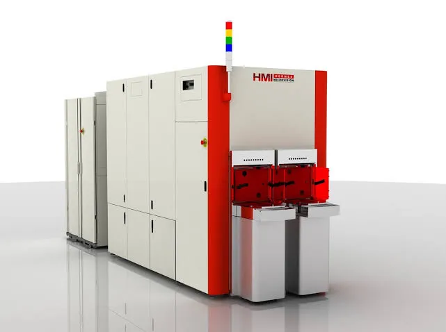
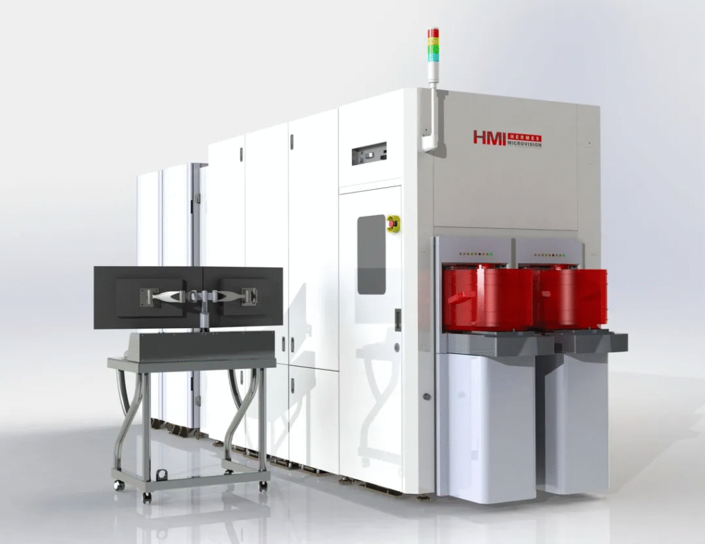
- eScan 430: Used for process development and production monitoring of 3D NAND and other advanced chips. It can operate in continuous scan and hot spot modes, detect physical defects and electrical faults below 10nm, and scan up to 1000 square millimeters per hour for voltage contrast inspection, allowing chip manufacturers to collect more data about their production processes and wafer performance. Key patents related to eScan 430 include TW (CN) I791197B and EP4123683A1.
- eScan 600: Can be used for physical defect detection in backscattered electron (BSE) mode, voltage contrast defect detection, and material contrast defect detection. It can detect physical defects as small as a few nanometers and features GDS (graphic design system) assistance, supporting online die-to-database (D2DB) inspection. Its unique large field of view (120μm x 120μm) enhances throughput in jump-scan mode without compromising sensitivity. Key patents related to eScan 600 include US20160314572A1, US20190333205A1, CN112313769A, and TW (CN) I794701B.
- eScan 1000: First introduced in May 2020, it is the first multi-electron beam (multi-beam) wafer inspection system, employing a 3×3 array of 9 electron beams. This increases throughput by approximately 9 times compared to a single electron beam while keeping crosstalk between beams to a minimum. It can be used for physical defect detection and voltage contrast defect detection. Key patents related to eScan 1000 include CN108885187B, CN113646865A, and EP4117014A1.
- eScan 1100: The first multi-electron beam (multi-beam) wafer defect inspection system for inline defect inspection, providing 15 times the throughput of a single electron beam inspection tool through 25 beams. Advanced Charge Control (ACC) and High-Voltage Injection (HVI) technologies offer comprehensive charge control capabilities, enabling the detection of electrical defects (including open, short, and leakage defects) and pattern defects down to 7nm. Key patents related to eScan 1100 include CN111164727A, CN112840432A, EP4001903A1, and CN116457652A.
- eP5: ASML’s highest-resolution electron beam system to date, with a pixel size of 1nm, capable of detecting defects smaller than 5nm, achieving <0.1nm CD precision and 0.05nm measurement sensitivity. The eP5 provides Automatic Defect Classification (ADC) and utilizes a large field of view (12000×12000 pixels) for high scanning throughput. Additionally, the eP5 can perform CD metrology and wafer inspection simultaneously to maximize productivity. Key patents related to eP5 include CN110998463A, US20190370950A1, CN112424826A, and CN113874787A.
Overlay error metrology is ASML’s most active innovative technical branch in the metrology and inspection domain, accounting for the highest proportion of applications. In terms of patent布局, it has developed three main routes from a foundational patent: measurement systems, overlay marks, and calculation methods. Current technological development focuses on improving detection beams, adjusting asymmetry, designing overlay marks, and improving models and optimizing/correcting parameters. Its product devices are mainly the YieldStar series, which optimize measurement wavelengths and reduce metrology costs through continuous wavelength selection and customizable measurement light bandwidth. They also reduce measurement acquisition time through faster sensor designs and enable simultaneous multi-layer measurement using in-device chip features or small metrology targets embedded in the chip design, thereby increasing measurement throughput.
Wafer defect inspection became a key branch for ASML in metrology and inspection after 2016, with a significant increase in application volume. In terms of patent布局, electron-based inspection has the most applications, focusing on improving speed, accuracy, and effectiveness. Scattering-based inspection has relatively fewer applications, with improvements mainly related to detection methods and optical paths. In terms of algorithms, the focus has shifted from precisely identifying defects from images to automatically classifying defects to improve productivity and, more recently, to reducing computational costs. Its HMI series products are all electron-beam wafer inspection tools.
ASML’s development experience offers valuable insights for Chinese semiconductor equipment R&D and sales companies. First, it’s crucial to accurately assess and grasp new technology trends. Once a company has established a certain position and accumulated experience in its mainstream technology and business, it can further strategically patent related technologies (such as metrology and inspection) around its core mainstream technology. In the initial stage of this布局, it is vital to identify valuable foundational patents and consistently invest in R&D, combining this with patent transfers to rapidly acquire relevant patents, laying the groundwork for building a strong patent portfolio. Second, companies can collaborate or merge with leading technology companies to form strong alliances, combine strengths, and complement each other, thereby building competitive resistance. Finally, fostering talent teams, especially team leaders, is essential. Enhancing inter-team collaboration while maintaining the stability of R&D teams and improving professional capabilities will promote sustainable R&D.
